|
|
|
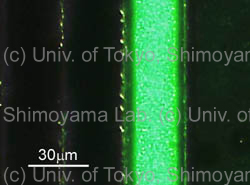
We demonstrate 30 µm-pitch OLED (Organic Light Emitting Diode) stripes, whose cathode was patterned by a lift-off method and was selectively addressable. The OLED consists of ITO (120 nm) - αNPD (70 nm) - Alq3 (70 nm) - Al (20 nm) - Au (1 nm) layers on a glass wafer (12 mm × 12 mm × 0.5 mm). A 2 µm-high convex stamp of the electrode pattern was formed from a Si-wafer by dry-etching, and it was pressed on the unpatterned surface of the OLED metal layer. The unwanted metal was removed because the metal layer was adhered to the convex of the Si-stamp, and a fine cathode pattern was formed.
References :
Takashi Hasegawa, Kiyoshi Matsumoto, Isao Shimoyama, “30 µm-pitch Stripes of OLED Patterned by Stamping Lift-Off Method,” 16th IEEE International Micro Electro Mechanical Systems Conference (MEMS '03), pp. 546-549, Kyoto, Japan, Jan. 19-23, 2003. [Proceedings]
Kazunori Hoshino, Takashi Hasegawa, Kiyoshi Matsumoto, Isao Shimoyama, “Organic Light-Emitting Diode Micro Patterned with a Silicon Convex Stamp,” Sensors and Actuators A, vol. 128, no. 2, pp. 339-343, 2006. [Paper]
|